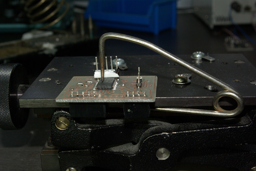
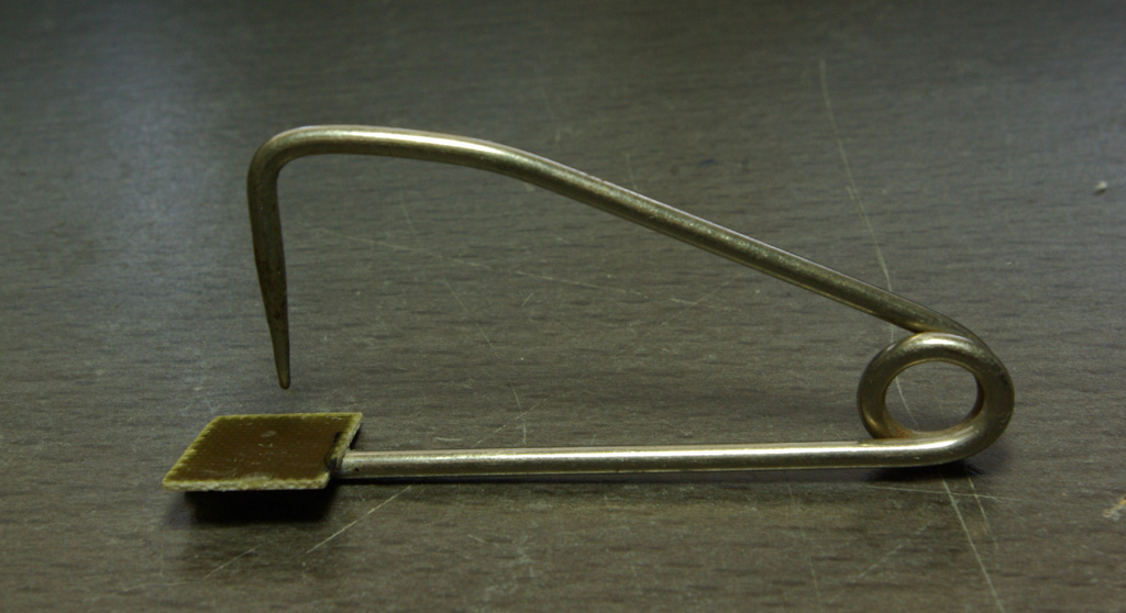
IC Clamp. Made from a very large ancient safety pin (these can sometimes be found on certain stands at rallies. They were probably used for mail sacks when these were made from hessian and carried on steam trains).
Cut off the head and bend the point round to 90 deg as shown. Solder on a small square of PCB to give some lateral stability and keep the point pressing down vertically.
Or bend-up a piece of steel wire such as galvanised fencing wire
This is how I solder small Quad Flat Pack devices with no tabs. Use a decent high magnification viewer; at least a headband type or for even greater magnification an old 50mm SLR camera lens is ideal. The pads on the PCB for the chip should first be tinned, aiming to keep an equal thickness of solder on each pad. Then the pads should be liberally coated with flux. Double, triple and quadruple check the IC alignment, place it central over the footprint so an equal amount of pad is showing on each side. Make sure there is flux still there on each pad. Press the IC down firmly, checking again for alignment. Look away for a few seconds, return and check alignment again.
Once absolutely certain each IC connection is above its pad, using a medium-sized (typically 1mm) soldering-iron bit place it in turn on each pad close to the IC, while watching the solder melt under the IC connections. The flux will cause a sort-of wicking action, drawing molten solder up from the pre-tinning to fill the gap and to fix at least some of the IC connections. Gently prod it make sure the IC is now fixed by at least some pads and won’t move of its own accord. Now apply more flux to the IC / PCB and load the soldering iron tip with solder. Wipe the iron against each side of the chip in turn, gently pushing solder into the gaps. Providing there is enough flux present, it should nicely flow into the minute gaps between each IC connection and its PCB pad. The flux – somehow, if there’s enough of it – always seems to prevent unwanted bridges forming. These are more likely if there is not enough flux, or the solder on the bit has been allowed to get dirty and oxidised.
Once the chip appears to be fitted, breath a sigh of relief and get out the high gain magnifier. Look carefully at each joint making sure there is a continuous solder flow from PCB pad to IC connection. Check also that there are no bridges. Bridges can be removed using solder wick / braid, again making use of extra flux at all times to aid solder flow and cleaning.
After fitting the main chip, installing the rest of the components should be straightforward!
Soldering Small Chips Especially ones with an exposed pad underneath, The Pin-zero problem